About Us

Currently, INOR offers PhD and MSc (Optoelectronics) Research Mode program for the following areas i.e Nano Materials Fabrication and Characterization, Nano Materials and Devices, Nano Device and Packaging, Modelling and Simulation of Nano Optoelectronic Devices, Nano Integrated Systems, Solid State Lighting System and Nano Optics field. In addition, MSc in Nano-Optoelectronics Mixed Mode program is also offered.
INOR is also supported by strong collaborations with well-known national and international universities as well as industries, in particular with the 2014 Nobel Laureate in Physics, Prof. Dr. Shuji Nakamura from the University of California Santa Barbara, on the technology transfer program related to GaN on GaN based LED research. We are ambitiously looking for future collaborations with more universities as well as industries in our niche areas: Nano and Advanced Materials, LED/Laser, Sensors, Solar Cell and Power Devices.
I
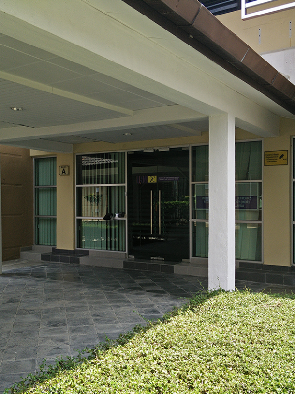
nstitute of Nano Optoelectronics Research and Technology (INOR) focuses on research and development (R&D) from the areas of nanoscience, nanomaterials, nanofabrication and nanoengineering that are collectively building intellectual and technological bridges from nanoscale concepts to practical nano optoelectronic devices and systems.
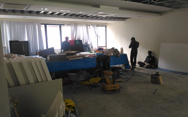
This institute has been considered to be one of the most modern and innovative research laboratories on optoelectronic and nanotechnology in Universiti Sains Malaysia which has an extensive range of equipment and facilities for growth, fabrication and characterization of optoelectronic and electronic devices at nanoscale. The physical structure and construction of the new laboratory are estimated to be worth RM 3 million (~USD 0.7 million); the equipment and facilities have cost another RM 15 million (~USD 3.5 million) and total floor area of approximately 300 m2.
The growth and fabrication equipment such as Metalorganic Chemical Vapor Deposition (MOCVD), E-beam evaporator system, Maskless Lithography system, Inductive Couple Plasma Etching System (ICP), Rapid Thermal Processor (RTP), Single Zone Tube Furnace and High Temperature Furnace are capable to produce nanoscale thin films and devices. Meanwhile the nanoscale characterization tools such as Electroluminescence, High Resolution X-Ray Diffraction (HRXRD), Photoluminescence Spectroscopy System, Optical Microscope, Probe station for Quick test, Probe Station with Micro-Positioner, Capacitance-Voltage/Current-Voltage (CV/IV) measurement systems are properly equipped to give the best results of morphology, structural, optical, and electrical properties of the materials.

