
Light-emitting diodes (LEDs)
Ultraviolet light emitting diodes (UV LEDs) or scientifically termed as aluminum gallium nitride-based UV LEDs (AlGaN based UV LEDs) have led to advancement in various applications, especially for bacteria and virus disinfection. However, most of the UV LEDs in the market today are only fews percent efficient. Hence, hinders their wide applications. One of the pre-requisites to improve the LEDs efficiency is to grow the LEDs on aluminum nitride (AlN) layers with a low threading dislocation density (TDD) . In principle, the threading dislocations (TDs) in the AlN layers can propagate into the active region of the overgrown LEDs, creating non-radiative recombination centers which significantly decrease the overall LEDs efficiency.
Solar cells
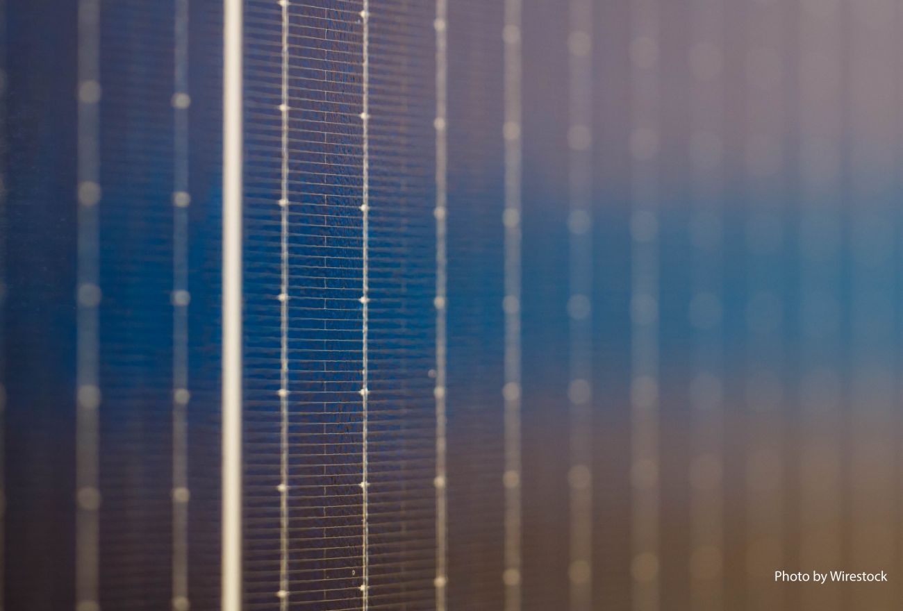
Silicon solar cells dominate more than 90% of the current PV market due to its abundance (in the form of silicon dioxide, SiO2), increasing conversion efficiencies, reducing technology cost (US$/Wattp) and proven stability after deployment . To date, the efficiencies of passivated emitter rear cell (PERC) silicon solar cells have reached around 26% under standard test conditions (STC). Crystalline silicon (with band gap of 1.12 eV) exhibits theoretical efficiency limit at 29%, as calculated by Shockley-Queisser model for a single junction solar cell. The theoretical efficiency is limited by thermalisation of hot electrons, below band gap photons and other losses. To improve the efficiencies of the silicon solar cells to beyond 29%, a tandem structure involving a solar cell (i.e. top cell) with a wider band gap semiconductor material is needed to ensure the whole spectrum of the sunlight (air mass, AM1.5G) is efficiently absorbed.
Nanophotonic devices
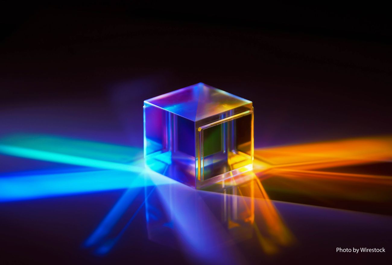
The convergence of electronic and optoelectronic components marks a novel technological paradigm, and within this landscape, III-nitrides emerge as frontrunners. The compounds of III-nitrides, including GaN, InN, and AlN, have garnered considerable attention in the realm of photonic devices, owing to their exceptional physical properties. A key attribute of III-nitrides is their direct energy band-gap, a feature that significantly reduces optical attenuation in comparison to indirect bandgap semiconductors like SiC, leading to heightened efficiency in photon emission and absorption . These materials boast a range of advantageous properties, such as a broad transparency range, high second-order non-linear optical coefficient, low thermo-optic coefficient, and resilience in harsh environments, making them ideal for photonics devices that manipulate light on microchips .
Power devices
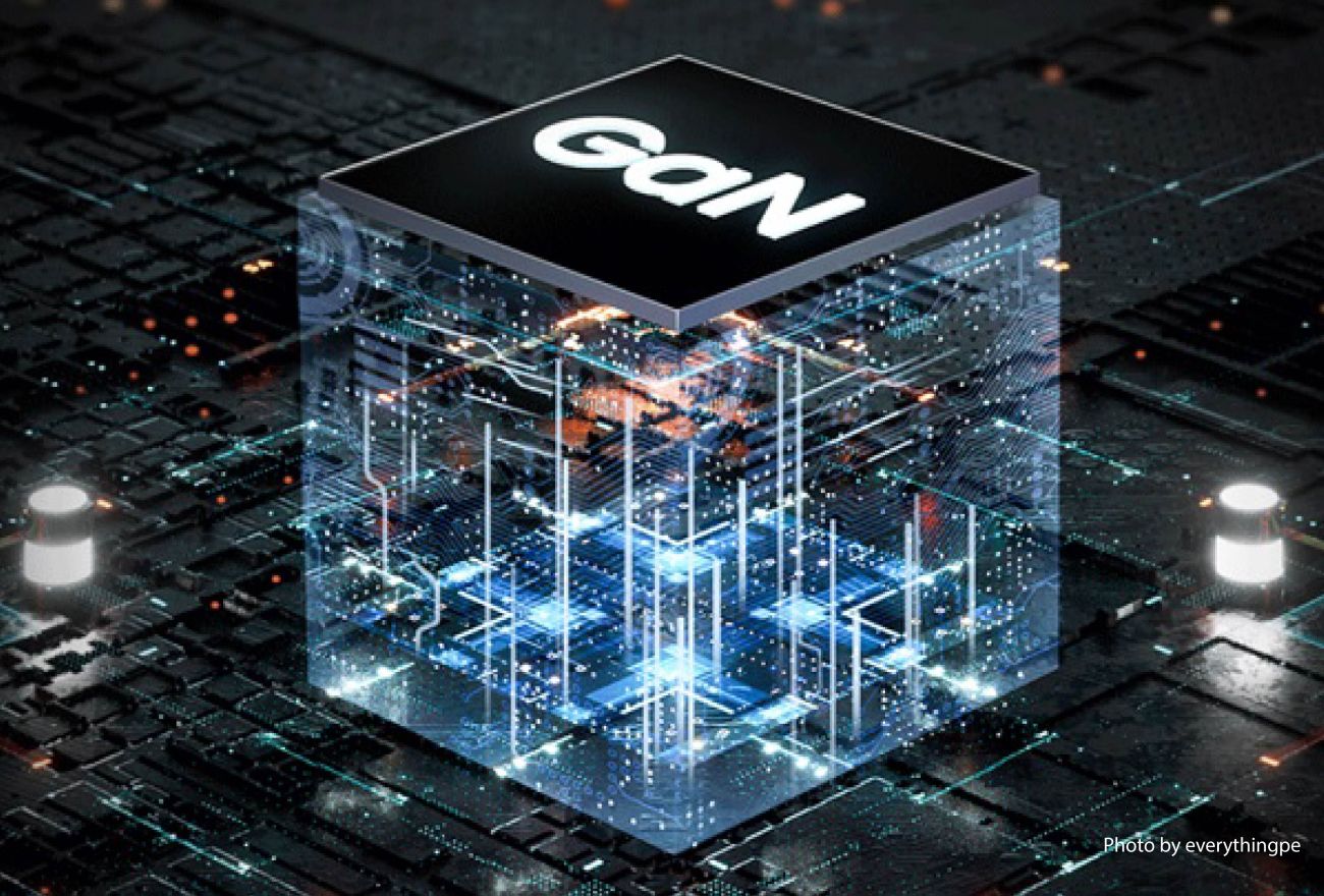
Gallium nitride high-electron-mobility transistor (GaN HEMT) has piqued the interest of researchers as a power device due to its high electron saturation velocity, reduced on-state resistance, high operating frequency and high breakdown voltage. These factors are attributed to the high electron mobility and high carrier concentration capability of GaN-based HEMTs. These merits are vital for a wide range of high-power and high-frequency applications, specifically for harsh-environment power electronics such as military, automotive, aviation, and space applications. Aluminium gallium nitride/gallium nitride (AlGaN/GaN) HEMT technology offers exceptional current density and output power devices and is poised to become the dominant technology in the near future.
UV Photodetectors
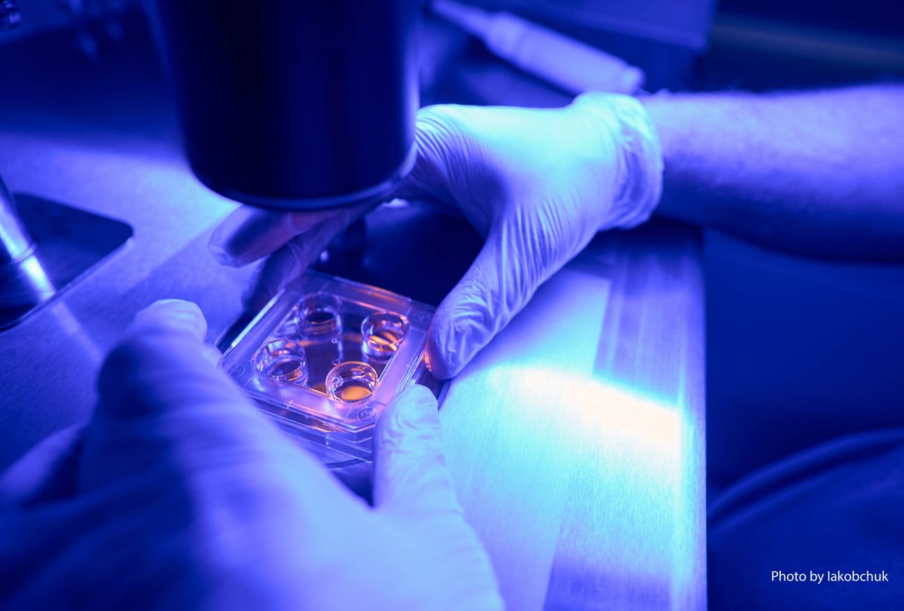
In recent years, there has been an increased interest in the development of ultraviolet (UV) detectors due to the increased demands in civil and military applications, space exploration, and space trips/tourism. At the same time, in the post-COVID-19 pandemic era, the use of UV light sources for the disinfection of viruses is expected to spike high. Since exposure to UV light can harm our health, this has stimulated the development and integration of UV detectors in our home appliances for fast UV detection. The current technology of UV detectors is still led/dominated by silicon (Si) -based UV detectors . However, due to its low band gap and low radiation resistance, it has limited applications, especially in harsh environments and outer space. UV-enhanced Si detectors with optical filters to reject the visible/IR wavelength were designed to solve the above issues. However, these UV-enhanced Si detectors are more complex and have additional weight. Therefore, wide band gap materials with high chemical and thermal stability as well as good anti-irradiation stability are needed.