Nanophotonic devices
Project Leader
Associate Professor Dr. Mundzir Abdullah
In the domain of active optical devices, III-nitride semiconductors have demonstrated remarkable success in the fabrication of light-emitting diodes (LEDs) and laser diodes, exhibiting high radiative efficiency, particularly in the visible wavelengths. For passive optical devices like waveguides, resonators, and modulators, III-nitride materials are poised to deliver high-performance devices, especially in the visible and ultraviolet (UV) spectra [5]. Recent advancements in UV and visible integrated photonics have expanded the horizons for III-nitride photonics, opening avenues in biochemical sensing, Raman spectroscopy, beam steering, nonlinear optics, and quantum photonics [6], [7].
Despite these strides, the pursuit of high-performance III-nitride waveguides presents a formidable challenge. Unlike traditional photonic waveguides, the optical loss in GaN waveguides at visible spectral wavelengths is dominated by multi-photon absorption processes, grain boundary effects, and inherent n-type doping, leading to free carrier losses [3], [6]. Meeting the stringent requirements for applications like stimulated Raman scattering and comb generation necessitates waveguides with extremely low optical loss, adding a layer of complexity to the technical landscape [7], [8].
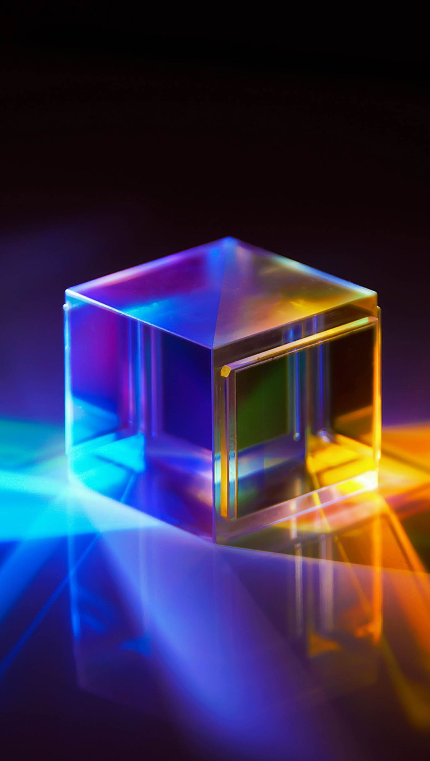
The unique properties of the III-nitride material system, including a wide transparency range, relatively high second-order nonlinear coefficients, and suitability for harsh environments, make it a promising candidate for integrated optics (IO) components and devices [1], [7], [9], [10]. Central to IO components are optical waveguides, the fundamental building blocks for modulators and switches. Achieving low propagation losses is pivotal for large-scale IO components and nonlinear optical devices. While various optical components have been demonstrated based on the III-N material system, the propagation losses in GaN waveguides have been reported to be higher than desirable, primarily attributed to the roughness of the etched sidewalls. Previous studies, using various techniques and designs, reported propagation losses of GaN based waveguides ranging from about 10 to more than 100 dB/cm. These values are much worse than the losses encountered when using Si or other III-V materials (e.g., GaAs and InP), which are a few tenths of dB/cm. Therefore, further utilization of the III-material system for IO and nonlinear optical devices, requires low loss waveguides [6].
Team Members
-
Dr. Sabah M. Mohammad
Universiti Sains Malaysia
-
Dr. Ahmad Syazwan Ahmad Kamal
Universiti Sains Malaysia
-
Ts. Dr. Muhammad Safwan Abd Aziz
Universiti Teknologi Malaysia
-
Associate Professor. Dr Chong Wu Yi
Universiti Malaya
-
Mr. Mohd Anas Ahmad
Universiti Sains Malaysia
-
Mrs. Rahil Izzati Mohd Asri
Universiti Sains Malaysia
Collaborators
-
Professor. Dr. Boon S. Ooi
King Abdullah University of Science and Technology (KAUST), Saudi Arabia
-
Professor. Dr. Philippe Boucaud
CRHEA-CNRS, France
-
Associate Professor. Dr. Jean-Jacques Delaunay
University of Tokyo, Japan